Description
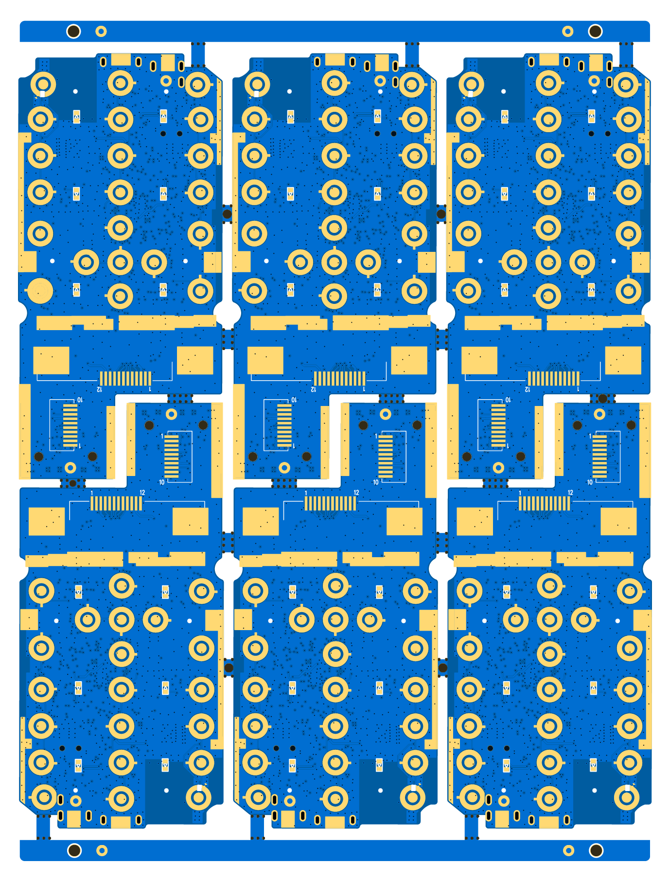
Multilayer PCB is a compact and efficient design tailored to meet the requirements of Walton feature phones. These PCBs incorporate advanced manufacturing techniques to ensure durability, performance, and reliability in compact electronic devices.
- Multilayer Design: Typically 4 layers to accommodate high-density interconnections.
- Material: High-quality copper-clad laminates (CCL) for signal integrity and heat resistance.
- Size Optimization: Ultra-thin profile to fit compact phone designs.
Manufacturing Highlights:
- Drilling and Routing: High-precision drilling for micro vias and smooth edge routing to meet design tolerances.
- Copper Plating: Uniform plating for conductivity and signal performance.
- Etching and Lamination: Ensures high precision for circuit pathways and robust interlayer bonding.
- Surface Finish: ENIG (Electroless Nickel Immersion Gold) for long shelf life and solderability.
- Quality Control: Rigorous electrical testing and AOI (Automated Optical Inspection) to eliminate defects.
This multilayer PCB ensures optimal functionality for feature phones by supporting seamless integration of processors, displays, and communication modules.


Reviews
There are no reviews yet.